
Chip stacking ‘3D packaging’
AI semiconductor technology will be in full swing next year Limitations of ultra-fine process to make chips smaller
‘3D packaging’ high performance and low power highlighted.
Market will grow to $78 billion by 2028. TSMC, Intel, etc. are racing to develop it
Samsung Electronics will begin its ‘3D packaging’ business next year, in which heterogeneous semiconductors are stacked vertically to operate as one chip. When chips are packaged vertically, data processing between semiconductors is faster and power efficiency is higher than when placed horizontally. For this reason, demand for 3D packaging from customers who want high-performance, low-power artificial intelligence (AI) semiconductors is increasing.
Verification of 3D packaging technology begins in earnest next year
According to the semiconductor industry on the 12th, Samsung Electronics will introduce 3D packaging using the semiconductor packaging technology ‘SAINT (Samsung Advanced Interconnection Technology)’ starting next year. Packaging is the process of connecting different types of chips to make them function as one chip. 3D packaging is characterized by stacking chips vertically, unlike regular packaging, which places chips horizontally.
Samsung Electronics has completed the technology verification of ‘SAINT-S’, which stacks SRAM, which serves as temporary data storage, on top of a processor such as a central processing unit (CPU). Next year, It is known that they plan to complete the technology verification of ‘SAINT-D’, which places DRAM for data storage on top of processors such as CPU and graphics processing unit (GPU), and ‘SAINT-L’, which places processors such as application processor (AP) above and below.
Used in chips for on-device AI
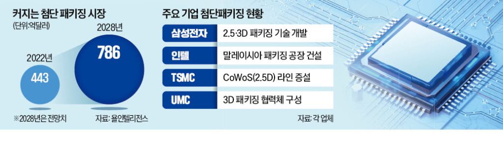
The reason Samsung Electronics is focusing on 3D packaging development is because the importance of the packaging process is increasing every year. Due to the limitations of ultra-fine processing technology that manufactures individual chips in small sizes, semiconductor companies are focusing on packaging that improves performance by properly arranging and connecting the manufactured chips. According to market research firm Yole Intelligence, the size of the high-tech packaging market is expected to grow from $44.3 billion last year to $78.6 billion in 2028.
Currently, 2.5D packaging is considered cutting-edge technology. 2.5D packaging is a horizontal arrangement of memory chips such as a processor and high bandwidth memory (HBM) on a packaging component called a ‘silicon interposer’. Chips are connected through silicon interposers. NVIDIA’s ‘AI Accelerator’ is produced through 2.5D packaging.
3D packaging places the chip top and bottom, so a silicon interposer is unnecessary. Instead, the chips are directly connected through TSV (through silicon electrode) technology. Since there is no need to connect chips side by side, space utilization increases and data processing speed and power efficiency can be improved through direct connection.
Demand for 3D packaging is emerging around cutting-edge semiconductors applied to generative AI and on-device AI. It is known that Samsung Electronics plans to use SAINT technology to improve the performance of semiconductors for AI data centers and APs for smartphones with on-device AI functions.
3D packaging is a measure of competitiveness
Samsung Electronics’ competitors, including TSMC, UMC, and Intel, are also active in launching cutting-edge packaging technologies and services. Taiwan’s TSMC is known to provide ‘SoIC’, a 3D packaging service, to chip production for Apple, Nvidia, etc. Intel is also using a 3D packaging technology called ‘Foveros’ to mass produce its latest chips.
Earlier this month, Taiwan’s UMC launched a 3D packaging collaboration project with domestic memory semiconductor company Winbond and No. 1 packaging company ASE. A semiconductor industry official emphasized, “Advanced packaging technology is becoming a measure of competitiveness,” and “Korea should also work to strengthen its packaging ecosystem.”