
“NAND controller order history, will be a weapon for targeting overseas markets”
“As the design field has become more specialized and changed, the role of design houses has expanded. A large part of the chip area is often designed by the design house.”
Design house, a big trend that cannot be resisted
The history of semiconductors is the history of the division of labor. As designs became more complex and astronomical amounts of capital were invested in production, design companies were divided into design companies (fabless) and production companies (foundries), and design companies were divided into fabless and design houses.
Design House is a company whose importance is growing as semiconductor design complexity intensifies. Although fabless designs chips, the main task is usually designing the chip’s algorithm. These design drawings rarely include details of the manufacturing process. Therefore, before manufacturing chips, it is necessary to create a blueprint for the manufacturing process again, and the design house is responsible for this process.
The design house serves as a bridge between fabless and foundry. At the time when semiconductor miniaturization was not severe, the existence of a design house was not necessary, but as miniaturization progressed, a design house specializing in blueprints for the manufacturing process became necessary.
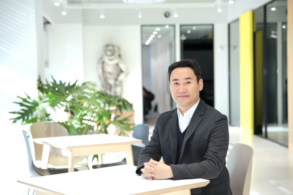
Joon-Gyu Park, CEO of AD Technology, said, “As the level of integration increases, there are more cases of joint design between fabless and design houses.” He added, “The importance of design houses has been emerging recently, and this is not a temporary phenomenon, but a long-term trend. “He said.
Recently, the scope of design houses has expanded to the front-end fabless. The reason is that demand for ‘application-specific semiconductors (ASICs)’ is increasing. (ASIC)’ refers to designing a chip to suit the user’s requirements.
Entering the 2010s, the semiconductor industry faces major limitations in its manufacturing process. The laws of ‘Moore’s Law’ and ‘Dernard Scaling’ no longer work. The laws of ‘Moore’s Law’ and ‘Denard Scaling’ no longer work. Moore’s Law means that the chip density improves twice every two years, and Denard Scaling means that as the size decreases, the performance improves. With complex designs and physical limits making it harder to boost semiconductor chip performance, companies are faced with one choice, which is to ‘choose and focus’.
Custom semiconductor refers to an attempt to overcome these physical limits by focusing on the performance you need. Tech companies like Google, Apple, etc. have succeeded in boosting performance once again by customizing semiconductors to their own situations and requirements, and the demand for custom semiconductors has increased exponentially.
The problem is that there are numerous electronic products and IT companies around the world, and there is no fabless company that can design chips to suit the requirements of all these devices and companies. As a result, there have been frequent cases of design houses penetrating the fabless space, and it has now become a trend.
CEO Park Jun-Gyu said, “It is nearly impossible to develop the system-on-chip (SoC) currently being developed independently due to the increase in complexity and scale,” and added, “The role of the design house has greatly expanded as the design environment changes. For example, he explained, “We provide a level zero service (a service that begins with discussing specifications with customers and designing them in the early stages of semiconductor design) according to the needs of the customer’s fabless company.”
Create a platform and prepare in advance
Amid these changes, AD Technology has thoroughly prepared to seize the opportunity. CEO Park Jun-gyu said, “The most important thing for a design house is the ability to read the market and make advance investments according to customer needs. In that respect, AD Technology has developed HPC (high-performance computing) and automotive platforms to strengthen its design capabilities over the past few years.”
He said, “In the case of system-on-chip for AI acceleration, which is currently being developed at home and abroad, it is very useful for product development by using the platform developed by AD Technology.” “We are developing it,” he explained. The process of designing a chip can be compared to the process of stacking Lego blocks. You can select and stack various blocks (IP/design assets) according to the shape you want to create. At this time, AD Technology provides fabless with a block (platform) with a certain shape. Fabless completes the shape by inserting the company’s own block (original IP) into the platform provided by AD Technology.
CEO Park said, “Looking broadly, the platform is also an IP asset. “Whether or not to own IP assets is made based on each design house’s strategic decision,” he said. “We predicted the growth potential of HPC and automotive and completed the related platform in advance. “Based on this, we are working to attract large fabless companies, such as overseas big tech companies, as customers,” he said.
CEO Park then said, “We are developing a customized foundation IP that could be a game changer.” Fabless designs a chip by taking the foundation IP (IP that serves as the basis for chip design) provided by a foundry. However, the desired power consumption and performance level are different for each fabless, which is difficult to implement with the general-purpose foundation IP provided by the foundry. For this reason, AD Technology provided customized foundation IP to help its customers, fabless, develop more competitive products. CEO Park said that AD Technology is currently the only domestic design house that provides customized foundation IP.
The NAND controller order history is weak… Talking with overseas NAND companies
Meanwhile, AD Technology is steadily accumulating technology by utilizing SK Hynix’s NAND controller order history and collaborating with affiliated companies to not lose memory design capabilities.
In the past, AD Technology had a history of winning orders for SK Hynix’s NAND flash controller when it was a partner company of TSMC, so it has strengths in the memory design field.
The controller is a system semiconductor that is installed in various storage devices using NAND flash memory and acts as the brain.
CEO Park said, “Recently, Chinese memory companies are preparing their own controllers, so we expect AD Technology’s (in memory design) experience to be used as a good weapon to target the Chinese market.”