
ADTechnology is a rare design house that understands all processes of the world’s top 1 and 2 foundries (semiconductor outsourcing production). Originally a value chain aggregator (VCA) of TSMC, it switched to Samsung Electronics’ Design Solution Partner (DSP) in 2019. This also means that it knows better than anyone else about the competitiveness of TSMC, a competitor of Samsung Electronics, and what Samsung Foundry needs to complement.
ADTechnology is taking on the role of a helper who will complement the weaknesses of Samsung Foundry, which has not been able to build a system semiconductor ecosystem as strong as TSMC. By growing intellectual property (IP) assets organization, it supports Samsung Foundry, strengthens its capabilities in high-performance computing (HPC) and automotive semiconductor design, and plays a role in attracting overseas customers to Samsung Electronics.
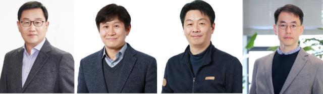
Yoon-seop Lee, ADTechnology’s Chief Strategic Marketing Officer, met with The Bell on 12th this month and emphasized, “Building on 15 years of experience as a TSMC VCA, combined with the capabilities of Samsung Electronics DSP leading in fine process technology, we have strengthened our differentiated competitiveness.” The three pillars supporting ADTechnology are System on Chip (SoC), platforms, and the infrastructure sector. The three departments collaborate individually and organically when necessary. At the new office in Pangyo 2 Techno Valley, the heads of the three departments, Lee Young-geun, Head of Infrastructure Division (Executive Director), Kim Seon-min, Head of Platform Division (Executive Director), and Park Seong-wook, Head of SoC Division (Executive Director), met in person.
◇ Infrastructure, customized foundation IP provided… Platform and SoC basic framework design
The infrastructure division led by Executive Director Lee Young-geun develops foundation IP (IP that forms the basis of chip design), namely standard cell libraries and S-RAM (cache memory) compilers. Fabless companies design chips by taking foundation IP provided by foundries. However, each fabless company has different desired power consumption and performance levels, making it difficult to implement with the general-purpose foundation IP provided by foundries. And because the foundry deals with so many customers, it is not easy to support all small and medium-sized fabless companies.
Executive Director Lee Young-geun emphasized, “By providing customized IP for customers, we help fabless companies develop more competitive products,” and stated, “The only domestic design house that can provide such foundation IP is AD Technology.”
Taiwan has a well-developed system semiconductor ecosystem, with many IP and library companies supporting TSMC, but in Korea, the ecosystem supporting Samsung Electronics is weak. Foundries that provide various IPs can be more attractive in the market. ADTechnology, recognizing the importance of IP, has established an infrastructure division after transitioning to DSP to complement Samsung Foundry.
Executive Director Lee Young-geun continued, “We completed the development of a standard cell library and SRAM IP for the 5nm (nanometer, one billionth of a meter) process that can improve Arm’s central processing unit (CPU) performance and performed MTO (tape-out). “The verification results will be released within the first half of the year,” he said. “Also, low power is an important factor in neural processing unit (NPU), a semiconductor for AI, and we are developing an SRAM memory library that implements low power, ultra-small size, and high speed, and will also be completed in the first half of the year.” “It’s going to happen,” he explained.
The platform division is a department that designs the SoC basic framework according to the specifications required by fabless. Executive Director Kim Seon-min said, “We are currently focusing on developing the Neoverse Computing System (CSS) platform for self-driving cars and servers.”
After the platform division or customer company completes the front-end design, the ball goes to the SoC division, which is responsible for the back-end design. Executive Director Park said, “Back-end design refers to the task of verifying whether the design meets the performance required by the customer, reflecting the foundry’s requirements, and then delivering it to Samsung Electronics for wafer production.” He added, “It is always right before moving to the foundry. “It has to go through our department,” he explained.
If a fabless customer wants Level-0 service (a business model that designs from the early stages of semiconductor design, from spec negotiation with customers to design), the platform division designs the platform first, then goes through the infrastructure and SoC divisions in order. Otherwise, it is covered only by the SoC division.
◇ Focusing on HPC·Automotive fields
ADTechnology is accumulating achievements in HPC, AI, and automotive-related orders. Last year, it achieved results in HPC SoC contracts based on 3nm and 4nm. It is also developing a 5nm-based SoC for autonomous driving in collaboration with Germany’s Videantis and domestic fabless company Bos Semiconductor.
Executive Director Lee Yoon-seop said, “The focus of the current era is on HPC and automotive,” and “It is very important to see what contracts a company is pursuing and the growth potential of that market. The fact that ADTechnology has strong capabilities in HPC and automotive chip design, which are expected to grow significantly in the future, means that there is a great potential for expanding contracts.”
High-performance chips for HPC and automotive applications often require highly complex designs. ADTechnology has differentiated itself in this field by possessing Big Die design capabilities. Executive Director Lee Young-geun emphasized, “One of AD Technology’s strengths is that it can provide Big Die solutions.”
A die refers to the individual unit of a semiconductor chip cut from a wafer. Big Die refers to designing chips that are large enough to fill a wafer. Executive Director Lee Yoon-seop said, “The larger the chip size, the more circuits are drawn, and the higher the design difficulty,” and “Companies with the capability to achieve Big Die are not abundant worldwide.”