
Japan is a strategic point for fabless and other companies to strengthen semiconductors with the Japanese government’s investment of KRW 90 trillion.
While the Japanese government is attracting global semiconductor companies such as TSMC and Micron with massive subsidies, Korean semiconductor companies are also speeding up their entry into the Japanese semiconductor market. This can be interpreted as an attempt to use Japan’s semiconductor reconstruction strategy as an opportunity to expand overseas and look for growth potential in the growing ecosystem.
Currently, major domestic semiconductor companies operating in Japan include Open Edge Technology, Telechips, and Gaon Chips. In particular, the Japanese market is considered a key point for expanding overseas sales for fabless (semiconductor design companies), IP companies, and design house companies that need to find new avenues within the still narrow domestic system semiconductor ecosystem.
Gaon Chips, a design house in charge of semiconductor design support, established a Japanese corporation at the end of 2022 and is expanding its business. As our first recent achievement, we signed a business agreement with Domain Devices, Japan’s largest semiconductor company. The design house serves as a bridge between the two by matching the blueprints created by the fabless to the foundry and providing technical support. The problem is that the domestic fabless market is still small and there is not much food. Therefore, Gaopchips targeted the Japanese market, where large set companies directly design semiconductors. We are working hard to collaborate with Sony, Panasonic, Toshiba, Fujitsu, and Renesas. Another advantage is that there are few design houses in Japan.
‘Telechips’, Korea’s leading automotive semiconductor fabless company, early established a branch in Japan and has been increasing the proportion of its sales in Japan. Last year, Telechips’ overseas sales accounted for 36.5%, of which the Japanese market reportedly accounted for a significant portion. The construction of this TSMC factory is expected to bring greater benefits as the semiconductor ecosystem in Japan is being revitalized.
‘Open Edge Technology’, Korea’s leading IP (intellectual property) company, established a Japanese branch in Yokohama last year and hired Takashi Yamada, a local semiconductor expert, as the general director (head) of technology sales and marketing. IP companies are companies that own intellectual property, such as specific technologies used in semiconductor design. It has fabless companies as its customers.
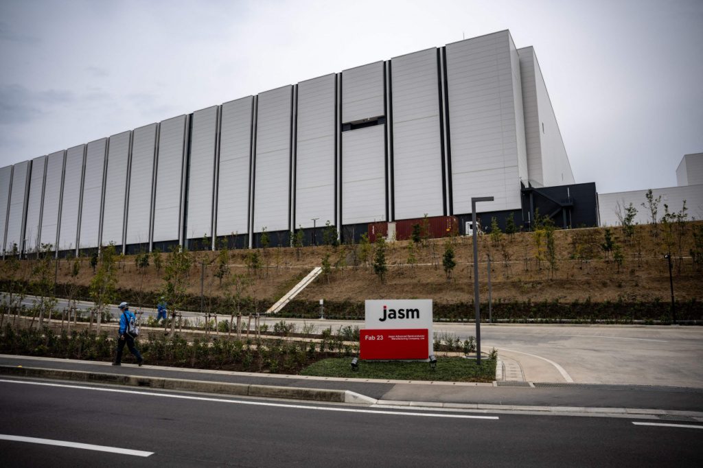
The Japanese government is investing $67 billion (about 90 trillion won) to revive the country’s semiconductor industry. Following the attraction of the TSMC factory, efforts are being made to recruit overseas fabless companies and support cutting-edge semiconductor R&D bases.
Samsung Electronics plans to invest more than 40 billion yen (approximately 363.7 billion won) by 2028, including establishing a new advanced semiconductor packaging technology research center, ‘Advanced Packaging Lab (APL)’ in Yokohama, Japan. It is scheduled to be built on a total site of 2,000 pyeong, and APL will pursue the development of semiconductor packaging and packaging technology. Japan’s Ministry of Economy, Trade and Industry provides support of up to 20 billion won.
As the importance of advanced packaging increases due to the AI semiconductor boom, the need for development of packaging technology is also increasing. Packaging refers to stacking multiple semiconductor chips vertically or connecting them horizontally. Packaging technology is also important for HBM (high bandwidth memory), a representative AI memory, and packaging is also used in the process of connecting it to a graphics processing unit (GPU) to make an AI semiconductor.
In order for packaging technology to advance, innovation in materials, materials, and parts and equipment used in the process is essential. This is why Samsung Electronics is establishing an R&D base in Japan, which is considered a powerhouse in the field of electronics and electronics.
jakmeen@heraldcorp.com