
AD Technology has won a project to support global companies’ design of 3nm ultra-fine process semiconductors. AD Technology’s first 3-nano project is expected to mass-produce Samsung Electronics’ semiconductor consignment production (foundry).
AD Technology announced on the 10th that it has signed a contract for a server-oriented semiconductor design project for overseas customers. Samsung Electronics is going to mass-produce it through ‘Gate All-Around (GAA)’ process, which is the world’s first next-generation transistor structure.
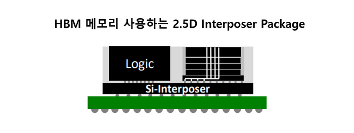
AD Technology also designs its own ‘interposer’ for advanced packaging and provides it to customers. The interposer is an element for parallel connection between semiconductors (dies) and is a core technology of 2.5D packaging. The connection between artificial intelligence (AI) semiconductors and high-bandwidth memory (HBM), which has recently attracted attention, is also made through the interposer. This project is expected to be a representative example of the expansion of the technology base to the packaging area, unlike the existing design houses that focused only on semiconductor circuit design.
The company said that although competition between domestic and foreign design houses was fierce, it won the project as a result of its recognition of AD Technology’s capabilities, including sales volume, design personnel and infrastructure. AD Technology is a member of ‘Design Solution Partner (DSP)’, a design house partner of Samsung Electronics foundry division.
This contract is evaluated to have played a role in the fact that the yield of Samsung Electronics’ 3-nano process is on track. It is known that Samsung Electronics is currently mass-producing GAA-based 3-nano first generation (SF3E) with stable yield. Foundry yield is a key factor in semiconductor production and is an essential capability to secure a large number of customers. Samsung Electronics plans to mass produce the second generation process (SF3) next year based on its experience in mass producing the first generation.
Jung Ki-bong, Vice President of Samsung Electronics, said, “It will be a good precedent for cooperation between Samsung Electronics’ foundry division and ecosystem partners.” Jun-Kyu Park, CEO of AD Technology, said, “3nm and 2.5D design experience will be a big weapon that differentiates AD Technology from other companies in the future.”