
In the global semiconductor market, design house partners are beginning to be recognized as the key to success beyond being helpers. In particular, Taiwan’s TSMC, which is a huge mountain that Samsung Electronics must overcome and is the No. 1 foundry (semiconductor consignment manufacturing) market, is regarded as the biggest driving force that dominates 60% of the global market is the strong design house ecosystem formed in Taiwan.
According to the Taiwan Semiconductor Association, as of 2021, there are a total of 235 design houses in Taiwan alone. Among them, Global Union Chip (GUC), which is considered the world’s No. 1 design house, is also the largest partner of TSMC. Beyond acting as a bridge between fabless (semiconductor design company) and TSMC, GUC also attracts customers based on state-of-the-art processes and manages major customers.
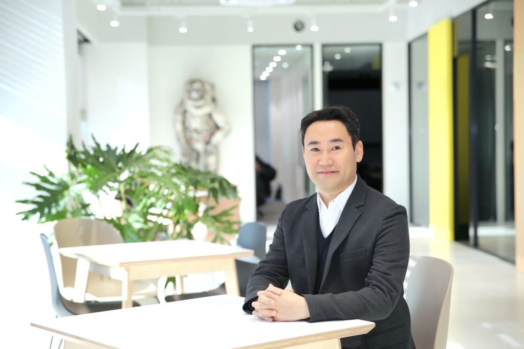
Mr. Park Jun Kyu, CEO of AD Technology, said in an interview with Chosun Biz on the 6th July, “Traditionally, design service partners, or design houses, have served as bridges for receiving designs from customers and passing them on to foundries, but now, the role of design houses has become much greater.” He said, “Because the chip has become too large and performs various functions, we are now conducting all processes from the design process together.”
Founded in 2002, AD Technology is a rare company that has experienced both TSMC and Samsung Electronics camps among design houses. It has been a partner of TSMC for 15 years since the establishment of the company, and since 2019 it has become one of Samsung Electronics’ largest partners. CEO Park explained, “I left TSMC because the strategies of AD Technology and Samsung Foundry matched while seeking the future growth potential of the company.”
Samsung Electronics’ foundry division has invested in a strong design house ecosystem to compete with TSMC and has been bearing fruit one by one since last year. Just as TSMC’s partners attract various customers from all over the world and bring them to TSMC, AD Technology also began winning major orders in various fields such as automotive, edge, and high-performance computing (HPC) from the end of last year. This is a sign that Samsung Foundry has entered into a virtuous cycle structure that it has been aiming for.
Unlike other design houses, AD Technology possesses next-generation technology capabilities such as 3D packaging as well as direct cutting-edge process design. CEO Park said, “The AD Technology Research Center directly operates a department specialized in manufacturing, and directly handles advanced processes such as 5-nano and 7-nano processes.” “We pride ourselves on being at the forefront of the field.” The following is a Q&A with CEO Park.
– Please explain about Design House and AD Technology.
“Since I founded the company in 2002, I think I am at the level of a college student now. All of the key personnel are from Samsung Semiconductor, and have worked with TSMC for about 15 years since its founding. Afterwards, in 2019, we started working as a design service partner (DSP) for Samsung Foundry. As it switched to Samsung Foundry, it focused on AI, edge, and automotive. The customers of design houses are usually fabless (a company specializing in semiconductor design), system semiconductor companies, or companies that directly develop magnetic semiconductors. As chips get bigger and their functions become more diverse, many engineers are needed in the manufacturing process. It has become difficult to implement all the ideas or algorithms that customers want with chips. This is why the role of design houses has grown. As chip sizes have become so large and diversified, design houses are now involved in everything from the design process.”

– Why did you leave TSMC and choose Samsung Foundry?
“I was deeply troubled. The size of the company needs to be increased, but in the TSMC ecosystem, I thought that it would either maintain the status quo or become smaller. In the end, a big decision was made. In particular, at that time, Samsung Electronics was strategically developing its foundry business. As the company’s founding members were from Samsung, they knew Samsung well, and Samsung Electronics was aggressively expanding its design house partners by referring to TSMC’s strategy. AD Technology also had experience as a TSMC partner. A number of conditions were well matched at the right time.”
– What are the characteristics of AD Technology as a design house?
“Our competitive edge and our future direction is to make chips with more energy efficiency. Unlike other design houses, AD Technology has many clients in the automotive, edge, and supercomputing fields. The trait they most want to have is sexual ratio. AD Technology has also been aiming for that part since its founding. AD Technology’s technology is that it has a built-in solution that can demonstrate a 5% to 10% overall performance ratio compared to other companies with a specialized foundation library. Paying the same development cost and producing the same performance, but with higher power efficiency.
Another strength is that the level of cooperation with ARM is very high. By developing a platform based on ARM’s design, it helps customers design chips easily. For example, if there are usually 300 engineers required to make a specific chip, AD Technology helps develop it in-house with less than 50 people. This is made possible through the strong partnership between AD Technology and ARM.”
– Samsung Electronics’ largest design house partner. Is the performance connected to the business success of Samsung Foundry?
“It is to add added value to the foundry’s basic competitiveness. From the Samsung Foundry’s point of view, preparing technology for customers is quite helpful. In the case of TSMC, most of its customers are not directly managed by TSMC, but by design houses. The most important point here is that the design house plays a role in developing semiconductors with higher characteristics by adding added value to the capabilities of the foundry company. Since 2019, efforts have been made to create a virtuous cycle structure like TSMC, and it has been bearing fruit since the end of last year. AD Technology signed a direct contract and began providing engineering. It is meaningful that we have increased the added value of the foundry through the design house.”
– Does the capacity of the design house affect the production speed or yield of the foundry company?
“AD Technology develops products together with a thorough understanding of the design that customers want. Many variables are considered before directly producing chips. A lot of know-how is required in the process where such engineering is preceded, and there are definitely parts that can contribute to yield.
Design houses play a large role in terms of cost and speed of developing chips. Chips in well-prepared fields can be used as they are. If necessary, the design desired by the customer can be provided as if assembling Lego blocks. If we develop chips like this, we can accelerate the speed by as little as six months and as much as three years.”
– What are your achievements since joining the Samsung camp to date?
“For the first two years after leaving the TSMC camp and joining Samsung Electronics, we focused on understanding the Samsung Electronics process. Now, we judged that we could win a contract directly to some extent, and the contract we won was for an automotive system-on-chip (SoC) company in Europe last year. Since then, it has also won orders for large-capacity server products. The product was a product that had to catch both the power ratio and performance.
At the recently held Samsung Foundry Forum, there were discussions on memorandum of understanding (MOU) related to development with US customers or more meaningful cooperation discussions. Contracts for 3-nano-based HPC are also expected to be signed soon. Winning the 3nm contract is significant. It is a chip that is large enough to fit in the palm of your hand worldwide and is a highly sophisticated technology that all engineering methodologies are put into.”