
Samsung Electronics and Taiwan’s TSMC are planning to enter competition by starting mass production of the second generation 3 nanometer (mn) process within this year. The two companies are noteworthy in that they will produce chips in the next-generation process in about two years, following the first-generation 3-nano process in 2022. The second-generation 3-nano process is expected to have an impact on securing large customers depending on whether it improves yield as well as performance.
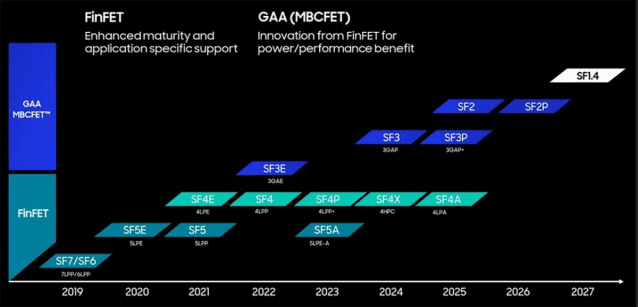
Samsung Electronics began mass production of the world’s first 3-nano (SF3E) process in June 2022, and is planning to mass-produce the second-generation 3-nano (SF3) process this year. According to information previously disclosed by Samsung Electronics at the ‘VLSI Symposium’, a global semiconductor conference held in Tokyo, Japan in May last year, the 2nd generation 3-nano process applied a gate-all-around (GAA) process that was more advanced than the 1st generation (SF3E).

As a result, the second-generation 3-nano process provides 22% faster performance, 34% improved power efficiency, and 21% smaller logic area compared to Samsung Electronics’ previous 4-nano FinFET process. Samsung Electronics is known to have secured a global server company as a customer in its second-generation 3-nano process.
TSMC also plans to begin mass production of chips in the second-generation 3-nano (N3E) process in the first half of this year and in the advanced 3-nano (N3P) process in the second half of this year, following mass production of the 3-nano (N3) process in December 2022.
According to TSMC, while the first-generation 3-nano (N3) process increased performance by 10-15% and reduced power consumption by 25-30% compared to the 5-nano process (N5), the second-generation 3-nano (N3E) process increased performance by 18%. It has been upgraded and power consumption has been reduced by 32%. Additionally, the N3P process improved performance by 5%, reduced power consumption by 5-10%, and increased chip density by 1.04 times compared to N3E.
TSMC is known to have secured Apple, MediaTek, AMD, NVIDIA, and Qualcomm as its second-generation 3-nano process customers. A representative example of the chip produced in the N3E process is the mobile processor (AP) ‘A18 Pro’ for the iPhone 16, which will be released in the second half of this year.
The 3-nano process is different in that Samsung Electronics adopted GAA, a next-generation transistor structure, while TSMC maintains the existing process, FinFET structure. Compared to the existing FinFET structure that covers three sides of the channel, GAA expands the gate area and is considered a next-generation technology that overcomes the decline in transistor performance due to process miniaturization and increases data processing speed and power efficiency. TSMC plans to apply the GAA structure starting from the 2-nano process.
An industry official familiar with Samsung Electronics’ foundry business said, “As a result of Samsung Electronics’ early introduction of GAA, the performance of the second generation 3-nm process has become more stable than that of the first generation. As cutting-edge processes are ultimately moving toward a GAA structure, Samsung has accumulated know-how first.” “The former may be advantageous,” they said.
This official also added, “If Samsung Electronics increases the yield in the second-generation 3-nano process, it will provide an opportunity for a ‘counterattack’ and engage in a real-life battle with TSMC.”
TSMC is also in desperate need of securing yield in its second-generation 3-nano process. So far, TSMC has received the full price of wafers from Apple only when the yield exceeds 70%, but when the yield of the first generation 3-nano process did not reach 70%, it signed a contract to sell only working chips (KGD, known good die). The interpretation is that TSMC decided that it was better to maintain large customers such as Apple even if it incurred losses.
An industry insider said, “It is an unusual case that TSMC signed a contract last year by charging Apple only for good-quality chips without charging the price per wafer input due to the low yield of 3-nano.” He also added, “TSMC also set the yield of the 2nd generation 3-nano process. “We will aim to secure multiple customers in addition to Apple.”
Meanwhile, Samsung Electronics and TSMC aim to mass produce chips based on the 2-nano process starting next year.
Samsung Electronics plans to mass produce a 2-nano process (SF2) focusing on mobile in 2025, expand to a high-performance computing (HPC) process in 2026, and automotive process in 2027. The 1.4 nano process is targeted for mass production in 2027. TSMC plans to introduce the 2-nano process (N2) next year and the upgraded 2-nano processes N2P and N2X in 2026, respectively. In addition, Intel also joined in and set a goal of mass production using the Intel 20A (2-nano grade) process in the second half of this year and the Intel 18A (1.8-nano grade) process next year.